
Selecting reliable Ceramic Injection Molding Semiconductor Components suppliers requires more than comparing prices or catalog photographs. Semiconductor components face demanding conditions, including thermal cycling, chemical exposure, tight dimensional limits, and strict contamination control. A strong supplier should demonstrate controlled ceramic powder preparation, stable feedstock formulation, precise molding, and validated debinding and sintering processes.
Randall M. German, a widely recognized powder injection molding expert, has emphasized, “The feedstock determines the success of powder injection molding.” This principle remains highly relevant. In practice, a small change in binder content can affect shrinkage, warpage, or surface quality. A poorly controlled furnace profile may leave discoloration near a thin wall. These details matter.
The leading Ceramic Injection Molding Semiconductor Components suppliers combine engineering experience with measurable process discipline. Their capabilities may include alumina, zirconia, aluminum nitride, and other technical ceramics. They should provide material certificates, lot traceability, dimensional inspection records, and realistic tolerance data. Clean manufacturing areas are also important, especially when components support sensitive semiconductor assemblies.
This article outline examines supplier expertise, ceramic materials, tooling design, molding accuracy, debinding reliability, sintering control, and post-processing capacity. It also considers technical communication, prototype support, production scalability, and quality-system evidence. A supplier may present excellent equipment yet lack consistent batch performance. That deserves scrutiny.
No supplier is perfect. Even experienced manufacturers can face yield variation during scale-up. Buyers should request samples, review test methods, and compare actual production data. The best decision is not based on impressive claims alone. It is based on repeatable evidence, transparent communication, and components that perform reliably inside demanding semiconductor environments.
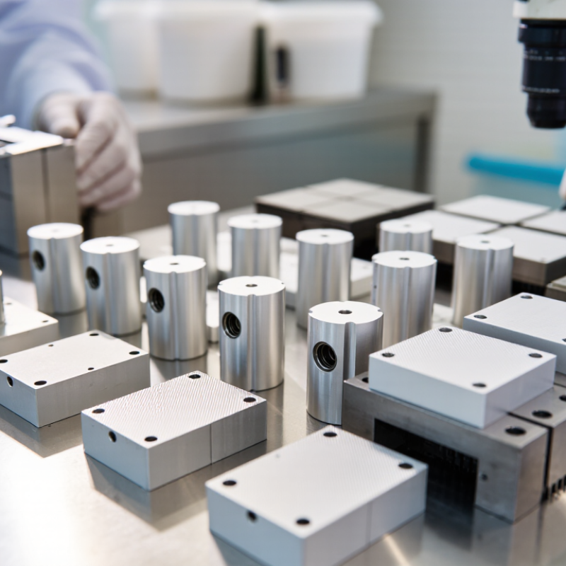
Ceramic Injection Molding in Semiconductor Component Manufacturing
Ceramic Injection Molding in Semiconductor Component Manufacturing
Ceramic injection molding produces precise semiconductor components with complex shapes and thin walls. The process starts with a ceramic powder, binder system, and carefully controlled feedstock. After molding, debinding removes the polymer gradually. Sintering then creates the final density and strength.
In practical production, temperature uniformity matters greatly. Uneven heating can cause cracks, warping, or hidden internal stress. Engineers inspect dimensions, surface finish, porosity, and dielectric performance. They also review batch records and material traceability. A reliable supplier should provide process validation, inspection data, and controlled packaging for clean manufacturing environments. Small gates can leave marks. Those marks may affect later assembly.
Tips: Confirm the component’s shrinkage model before tooling. Request sample data from multiple production lots. Check how the supplier controls debinding time, furnace atmosphere, and final inspection. A design that looks perfect on paper may still require adjustment after sintering. That lesson is easy to overlook.
Experience shows that ceramic injection molding rewards stable processes rather than rushed optimization. Tool wear, powder variation, and moisture can slowly change results. Regular equipment checks help maintain consistency. However, no process is completely flawless. Careful feedback between design, molding, and quality teams remains essential for dependable semiconductor component manufacturing.
Top Ceramic Injection Molding Semiconductor Components Suppliers - Ceramic Injection Molding in Semiconductor Component Manufacturing
| Component Category | Typical Ceramic Materials | Key Semiconductor Applications | Important Performance Requirements | Common Post-Molding Operations | Supplier Evaluation Criteria |
|---|---|---|---|---|---|
| Insulating Feedthroughs | Alumina; high-purity alumina | Vacuum equipment, process chambers, sensor assemblies | High dielectric strength, low outgassing, dimensional stability, chemical resistance | Debinding, sintering, grinding, metallization, leak testing | Purity control, hermeticity testing, cleanroom handling, traceability |
| Insulator Rings and Spacers | Alumina; zirconia for high toughness | Wafer-handling equipment, alignment systems, electrical isolation assemblies | Tight concentricity, wear resistance, electrical insulation, low particle generation | Precision lapping, polishing, dimensional inspection | Tooling capability, shrinkage compensation, surface-finish control |
| Ceramic Nozzles and Gas Distribution Parts | Alumina; aluminum nitride for thermal conductivity | Gas delivery, plasma processing, cleaning and deposition equipment | Controlled flow passages, plasma resistance, thermal stability, low contamination | Drilling or machining of passages, polishing, ultrasonic cleaning | Internal-channel inspection, particle-control procedures, material certification |
| Electrostatic Chuck Components | Alumina; aluminum nitride | Wafer clamping and temperature-controlled processing | Dielectric uniformity, flatness, thermal conductivity, low leakage current | Surface grinding, electrode integration, metallization, electrical testing | Flatness measurement, electrical uniformity testing, thermal mapping capability |
| Ceramic Heater Substrates | Aluminum nitride; alumina | Wafer heating, chemical vapor deposition, etching and drying systems | High thermal conductivity, thermal-cycle resistance, uniform heat distribution | Thinning, polishing, conductor printing, brazing or bonding | Thermal uniformity data, bond reliability, flatness and warpage control |
| Plasma-Facing Components | Alumina; yttria; quartz-based ceramics | Etch chambers, plasma shields, liners and focus-ring assemblies | Plasma erosion resistance, low metal contamination, thermal-shock resistance | Precision machining, coating, surface finishing, particle inspection | Plasma compatibility data, coating adhesion, contamination-control history |
| Ceramic Packages and Headers | Alumina; aluminum nitride for thermal management | Power semiconductor modules, sensors, hermetic electronic packages | Hermetic sealing, electrical insulation, coefficient-of-expansion compatibility | Metallization, brazing, plating, helium leak testing | Package design support, metallization quality, seal integrity, inspection records |
| Precision Ceramic Tooling | Alumina; zirconia; silicon nitride | Assembly fixtures, alignment tools, inspection and handling equipment | High hardness, dimensional repeatability, low thermal expansion, wear resistance | CNC grinding, lapping, polishing, coordinate measurement | Measurement capability, tool-life data, repeatability studies, engineering support |
| Common Ceramic Injection Molding Workflow | Ceramic powder, thermoplastic binder system, processing additives | Complex, small and repeatable semiconductor component geometries | Uniform feedstock, controlled shrinkage, defect prevention, stable sintering | Feedstock preparation, injection molding, debinding, sintering, finishing | Process validation, mold-flow analysis, statistical process control, lot traceability |
| Quality and Compliance Indicators | Material grade and purity documented by lot | Semiconductor, vacuum, thermal and high-reliability applications | Particle control, dimensional consistency, chemical compatibility, reliability | CMM inspection, microscopy, density testing, electrical and leak testing | Documented quality system, inspection plans, corrective-action process, change control |
FAQS
It produces complex ceramic components with thin walls and precise dimensions. Common uses include insulators, fluid guides, wafer-handling parts, and high-temperature fixtures.
Alumina provides electrical insulation and chemical resistance. Aluminum nitride supports heat transfer. Zirconia offers toughness under repeated mechanical stress.
Ceramic powder mixes with a binder system to create controlled feedstock. Molding forms the part, debinding removes polymers, and sintering creates final strength.
Uneven heating can cause cracks, warping, and hidden internal stress. Furnace records should show stable thermal conditions across each production cycle.
They should inspect dimensions, surface roughness, porosity, flatness, sealing areas, and dielectric performance. Functional testing still matters.
Request pilot-run data from several production lots. Review powder storage, furnace uniformity, rejected parts, calibration records, and corrective actions.
Controlled packaging, documented cleaning, particle limits, ionic contamination checks, and outgassing evaluation are important. Traceability should cover every material batch.
No process is completely flawless. Shrinkage can vary after sintering, so tooling models and production evidence need regular review.
Small gates may leave marks affecting assembly. Poor debinding can create cracks, while powder variation or moisture may slowly change results.
A drawing can look correct before firing but fail afterward. Practical thermal, dimensional, and assembly tests may reveal overlooked adjustments.
Conclusion
Ceramic Injection Molding Semiconductor Components explores how ceramic injection molding supports the production of precise, durable parts for semiconductor manufacturing. By combining engineered ceramic powders with controlled molding and sintering processes, suppliers can create complex geometries, thin walls, and tight tolerances while maintaining excellent thermal stability, electrical insulation, chemical resistance, and dimensional consistency. Commonly produced items include insulators, sensor housings, wafer-handling parts, process tubes, feedthroughs, and other high-performance components used in demanding production environments.
When evaluating suppliers, manufacturers should consider material expertise, mold design capabilities, process control, scalability, inspection systems, and technical support. Advanced automation, clean manufacturing areas, precision machining, and reliable sintering technology can improve repeatability and reduce contamination risks. Quality certifications, traceability, statistical process monitoring, and application-specific testing are also important indicators of supplier reliability. These standards help ensure that ceramic components perform consistently in high-temperature, corrosive, vacuum, and high-purity semiconductor production applications.