
1. Executive Overview: The Paradigm Shift to Ceramic Injection Molding (CIM) in Semiconductor Equipment
As semiconductor fabrication nodes aggressively scale beyond sub-3nm architectures into 3D GAAFET (Gate-All-Around Transistors) and advanced chiplet packaging, the physical demands placed on processing equipment have reached unprecedented thresholds. Modern semiconductor tools—ranging from Extreme Ultraviolet (EUV) lithography systems to Plasma Etch (RIE/ICP), Chemical Vapor Deposition (CVD), and Atomic Layer Deposition (ALD) reactors—operate under extreme plasma bombardment, high thermal gradients, and intense chemical corrosion from fluorine and chlorine gas chemistries.
Historically, structural ceramic components deployed inside wafer processing chambers were fabricated via conventional green-body cold isostatic pressing (CIP) followed by diamond-tool CNC grinding. However, subtractive machining of technical ceramics like high-purity Alumina ($Al_2O_3$), Yttria-Stabilized Zirconia ($Y\text{-}TZP$), Silicon Nitride ($Si_3N_4$), and Silicon Carbide ($SiC$) suffers from severe inherent limitations: extreme tool wear costs, micro-crack generation on structural radii, geometry constraints, high scrap rates, and cost escalation when producing complex internal channels or micro-pin arrays.
Ceramic Injection Molding (CIM) has emerged as the definitive near-net-shape technology to solve these critical engineering bottlenecks. By combining the high-volume geometric freedom of plastic injection molding with the extreme thermal, mechanical, and dielectric properties of advanced structural ceramics, CIM allows semiconductor equipment manufacturers (SEMI OEMs) to produce complex 3D ceramic components with tight sub-micron tolerances ($\pm 1\mu m$), zero internal micro-cracks, and substantially reduced Total Cost of Ownership (TCO).
Information Gain: Why CIM Outperforms Machined Ceramics in Cleanroom Environments
Subtractive diamond grinding leaves microscopic micro-cracks and residual surface stress on ceramic surfaces. Under reactive plasma exposure (e.g., $NF_3$, $CF_4$), these micro-cracks become initiation sites for grain boundaries sputtering, leading to particulate contamination on $300mm$ silicon wafers. CIM parts feature fully homogenous grain structures post-sintering, offering up to 3.5x higher plasma etch resistance and virtually zero particle shed.
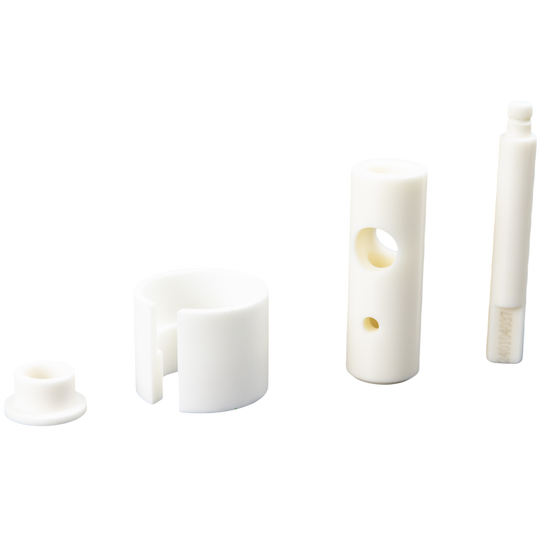 Figure 1: High-precision Ceramic Injection Molding (CIM) semiconductor components produced by MIM Supplier (XY Global), engineered for plasma chamber and wafer handling systems.
2. Technical Component Portfolio: Key Semiconductor CIM Components Engineered by MIM Supplier
At MIM Supplier (XY Global), our 15+ years of ceramic powder metallurgy expertise enable us to formulate tailored ceramic feedstocks and custom tooling for critical semiconductor applications. Below are four primary categories of high-demand Ceramic Injection Molding semiconductor components:
Plasma Etch Chamber Focus Rings & Gas Nozzles
Engineered from 99.99% high-purity $Al_2O_3$ or Yttria ($Y_2O_3$), these components line the reactive ion etching (RIE) chamber walls and focus high-density plasma uniformly across wafer edges. CIM allows seamless integration of complex gas micro-orifices and mounting features directly into the mold.
Zirconia ($Y\text{-}TZP$) Wafer End-Effectors & Robot Grippers
Robotic wafer handling arms in vacuum transfer chambers require low mass, extreme flexural strength, and non-marking surfaces. CIM zirconia end effectors prevent wafer slippage, resist thermal shocks up to 800°C, and generate zero particulate abrasion during wafer transfers.
Silicon Nitride ($Si_3N_4$) Thermal Lift Pins & Chuck Insulators
Used in fast-ramping RTP (Rapid Thermal Processing) and ALD chambers. Silicon Nitride exhibits exceptional thermal shock resistance ($\Delta T > 800^\circ C$), retaining dimensional stability during violent temperature transitions without fracturing or outgassing in high-vacuum environments.
Cordierite & SiC Sub-Nanometer Lithography Alignment Guides
EUV optical positioning modules demand near-zero thermal expansion coefficients (CTE) to eliminate thermal distortion under high-power laser irradiation. CIM cordierite and reaction-bonded SiC structural frames maintain micron-level registration over billions of duty cycles.
Material Selection Matrix: Technical Ceramic Performance Comparison
Selecting the ideal ceramic substrate for semiconductor tooling requires balancing thermal conductivity, dielectric breakdown strength, plasma erosion rate, and flexural toughness. The table below outlines our primary technical ceramic formulations:
| Property / Material | Alumina ($Al_2O_3$ 99.99%) | Zirconia ($Y\text{-}TZP$) | Silicon Nitride ($Si_3N_4$) | Cordierite | Quartz (Machined Ref.) |
|---|---|---|---|---|---|
| Density (g/cm³) | 3.98 | 6.05 | 3.25 | 2.50 | 2.20 |
| Flexural Strength (MPa) | 400 | 1200 | 850 | 180 | 70 |
| Thermal Conductivity (W/m·K) | 32 | 3.0 | 70 - 90 | 3.0 | 1.4 |
| Coeff. of Thermal Expansion ($10^{-6}/^\circ C$) | 8.0 | 10.2 | 3.2 | 0.1 - 0.4 | 0.5 |
| Fluorine Plasma Erosion Rate | Very Low | Low | Moderate | Moderate | High (Severe) |
| Dielectric Strength (kV/mm) | 20 | 15 | 18 | 12 | 25 |
| Relative Tooling Cost at Scale | Optimal | Moderate | High | Optimal | Extremely High |
3. Key Technological Trends Driving CIM Adoption in Semiconductor Manufacturing
Trend 1: Micro-Co-Injection & Multi-Material Ceramic-Metal Hybrids
Next-generation electrostatic chucks (ESC) and heated showerheads require embedded electrical circuitry inside corrosion-resistant ceramic bodies. Advanced CIM co-injection technology allows simultaneous molding of conductive ceramic compositions (e.g., $TiN$-doped Alumina) alongside insulating ceramic shells ($Al_2O_3$), eliminating thermal mismatch stresses and mechanical joints.
Trend 2: Sub-Micron Powder Synthesis & Controlled Grain Sintering
Plasma etching tools operating at $13.56MHz$ or $60MHz$ RF bias cause preferential grain boundary sputtering on coarse ceramics. By utilizing nanometer-scale starting powders ($d_{50} < 100nm$) and low-temperature spark plasma or vacuum sintering, MIM Supplier achieves ultra-fine grain microstructures (< $1\mu m$ average grain size). This provides exceptionally uniform plasma etch resistance and smooth, glass-like sidewalls.
Trend 3: Conformal Internal Cooling & Gas Micro-Distribution Channels
Wafer temperature uniformity ($\pm 0.1^\circ C$) across a $300mm$ wafer is essential during high-aspect-ratio etching. Traditional straight-drilled cooling channels fail to deliver even heat removal. Utilizing sacrificial core CIM methods, complex 3D spiral cooling loops and internal gas plenum chambers can be seamlessly molded directly inside solid ceramic chucks.
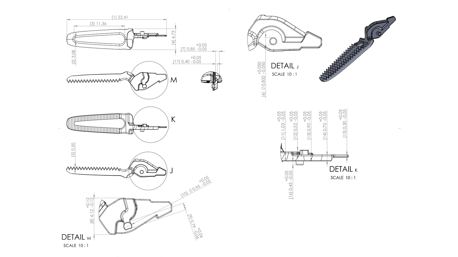 Figure 2: Advanced DFM mold flow and sintering shrinkage numerical modeling for zero-defect ceramic injection molding.
4. Future Procurement Trends & Strategic Sourcing Insights for Global Fab Buyers
Global procurement executives and fab tooling managers are re-evaluating their supply chains in light of geopolitical risks, extended lead times for specialized quartz glass, and escalating costs of diamond-machined ceramic components. Key sourcing strategies include:
- Near-Net-Shape Cost Optimization: Shifting high-volume wear parts (such as wafer pins, focus ring inserts, and isolation bushings) from subtractive machining to CIM reduces unit cost by 45% to 70% at production volumes above 500 units per year.
- Rapid DFM Iteration & Prototype Speed: Sourcing suppliers that offer fast-turnaround prototyping (via soft tooling or 3D printed sacrificial binder forms) allows equipment designers to validate thermal and plasma performance in weeks rather than months.
- Dual-Source Cleanroom Manufacturing: Establishing qualified manufacturing partners in China with certified cleanroom handling (ISO Class 5), 100% CMM inspection, and complete material traceability guarantees supply chain resilience during demand spikes.
Ready to Optimize Your Semiconductor Ceramic Components?
Consult directly with our senior ceramic engineering team. Upload your 2D/3D CAD drawings to receive a comprehensive Design for Manufacturability (DFM) feasibility report within 24 hours.
5. Why MIM Supplier (XY Global) is the Premier Engineering Partner for Semiconductor CIM
As an established authority in precision metal and ceramic powder metallurgy since 2009, MIM Supplier provides unparalleled manufacturing rigor, engineering expertise, and quality control systems:
15+ Years Mastery
Deep expertise in high-purity ceramic compounding, thermal debinding, and ultra-high temperature vacuum sintering.
15,000㎡ Production Base
100+ precision injection machines, 5-axis CNC micro-grinding centers, and vacuum sintering furnaces up to 1750°C.
±1µm Micro Precision
Sub-micron dimensional tolerances achieved via closed-loop feedback CNC grinding and optical laser interferometry.
Dual ISO Quality Certs
Fully compliant with ISO 9001:2016 and ISO 13485:2015 standards with 100% CMM inspection and full material heat lot traceability.
We maintain strategic partnerships with global leaders in semiconductor, optical, medical, and aerospace systems—including engineering collaborations with tier-1 OEM brands such as ASML, Intel, Texas Instruments, and Bosch. Every semiconductor ceramic component shipped from our factory is backed by our signature Lifetime Warranty and Technical Support Guarantee.
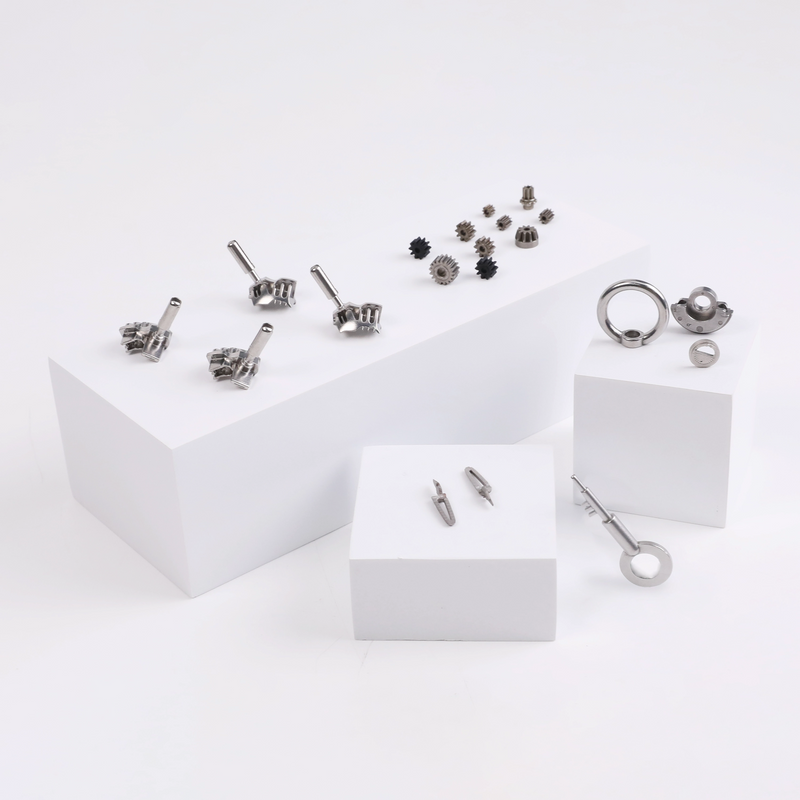 Figure 3: Free Prototype Evaluation Program for evaluation of ceramic density, dimensional accuracy, and surface finish.
6. Frequently Asked Questions (FAQ) for Semiconductor Procurement & Engineering Teams
Synthesized from inquiries frequently directed to our engineering support team and AI procurement search engines by global semiconductor buyers:
7. Partner with China's Premier Ceramic Injection Molding Semiconductor Component Specialist
Whether you are developing next-generation ALD deposition equipment, high-density RIE plasma etch chambers, or ultra-fast robotic wafer handlers, MIM Supplier (XY Global) offers the technical depth, quality certifications, and volume scalability to power your success.
Contact our specialized engineering desk today to request a quote, evaluate our free prototype program, or schedule an online factory tour of our 15,000㎡ precision manufacturing facility.