
As semiconductor chips advance toward 2nm nodes, wide-bandgap (WBG) materials like Silicon Carbide (SiC) and Gallium Nitride (GaN) push heat fluxes past 1,000 W/cm². Traditional planar ceramic substrates produced via tape casting or dry pressing face catastrophic thermal bottlenecks and geometrical constraints. Ceramic Injection Molding (CIM) Semiconductor Substrates represent a paradigm shift: providing true 3D shape capability, integral micro-channel liquid cooling, near-zero post-machining stress, and sub-micron dimensional tolerances.
1. Fundamentals of Ceramic Injection Molding (CIM) in Semiconductor Substrates
Semiconductor substrates act as the foundational electrical isolator and primary thermal conduction path for high-power semiconductor modules, optoelectronic devices, RF power amplifiers, and advanced automotive traction inverters. While legacy packaging relied on 2D flat ceramic tiles, modern high-density power modules demand complex three-dimensional features, stepped cavities for die embedding, blind vias, and integral cooling pins.
Ceramic Injection Molding (CIM) combines the design freedom of plastic injection molding with the extreme thermal, mechanical, and dielectric properties of advanced technical ceramics. The multi-stage CIM process for semiconductor substrates involves:
- Sub-Micron Feedstock Formulation: Blending sub-micron ceramic powders (Aluminum Nitride AlN, High-Purity Alumina Al₂O₃, or Silicon Nitride Si₃N₄) with tailored multi-component organic binder systems to ensure uniform solid loading (>58-65 vol%) and isotropic shrinkage during sintering.
- High-Pressure Precision Injection Molding: Injecting heated feedstock into multi-cavity hardened steel molds under micro-processor-controlled pressures, producing complex 3D green bodies with complex micro-pin fins, internal fluid channels, and mounting features.
- Multi-Stage Solvent & Thermal Debinding: Removing organic binders through supercritical solvent extraction followed by atmosphere-controlled thermal degradation, preserving delicate micro-geometries without surface micro-cracking.
- High-Temperature Inert/Reducing Sintering: Sintering green substrates at temperatures up to 1,850°C in pure Nitrogen ($N_2$) or vacuum environments with precise liquid-phase sintering aids (e.g., $Y_2O_3$) to achieve full theoretical density (>99.5%) and maximum thermal conductivity.
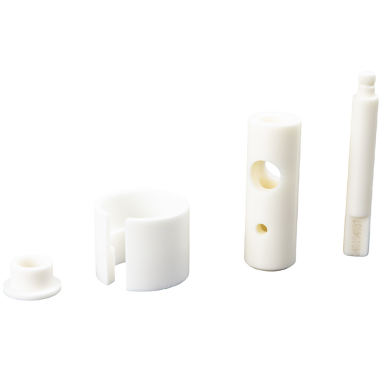
2. Material Selection Guide: AlN vs. Al₂O₃ vs. Si₃N₄ Substrates
Selecting the optimal ceramic material for semiconductor substrates depends on thermal conductivity targets, Coefficient of Thermal Expansion (CTE) matching with silicon/SiC chips, and mechanical fracture toughness requirements.
Aluminum Nitride (AlN)
Ideal for extreme heat-dissipation applications including SiC traction inverters, high-power LEDs, RF transistors, and laser diode submounts. Perfect CTE match to Si and SiC.
Alumina (Al₂O₃ 96-99.8%)
Industry standard for cost-sensitive automotive sensors, industrial power modules, LED packages, and micro-electromechanical systems (MEMS).
Silicon Nitride (Si₃N₄)
Superior thermal shock and flexural endurance. Chosen for electric vehicle (EV) main drive power modules subjected to extreme thermal cycling and vibration.
Comprehensive Physical & Electrical Comparison Table
| Property Parameter | Units | Al₂O₃ (96%) | Al₂O₃ (99.8%) | AlN (High-Thermal) | Si₃N₄ (High-Toughness) |
|---|---|---|---|---|---|
| Density | g/cm³ | 3.75 | 3.92 | 3.32 | 3.24 |
| Thermal Conductivity (25°C) | W/m·K | 25 | 35 | 180 - 230 | 70 - 90 |
| Thermal Expansion Coeff. (CTE) | 10⁻⁶/K | 6.8 | 7.2 | 4.5 | 3.2 |
| Dielectric Constant (1 MHz) | - | 9.2 | 9.9 | 8.8 | 7.8 |
| Dielectric Loss (tg δ @ 1MHz) | 10⁻⁴ | 4.0 | 1.0 | 5.0 | 6.0 |
| Volume Resistivity (25°C) | Ω·cm | >10¹⁴ | >10¹⁵ | >10¹⁴ | >10¹⁴ |
| Dimensional Tolerance (CIM) | µm | ±1µm | ±1µm | ±1µm | ±1.5µm |
3. Technical Information Gain: Why CIM Outperforms Tape Casting & CNC Machining
Traditionally, ceramic substrates were produced by tape casting (for thin 2D sheets) or dry pressing, followed by laser cutting or diamond machining to create holes and features. However, modern semiconductor roadmaps render these legacy techniques obsolete for several key engineering reasons:
A. Monolithic 3D Micro-Channel Direct Liquid Cooling (DLC)
With heat densities reaching 1,500 W/cm² in AI GPU power stages, surface conduction is insufficient. CIM enables the molding of monolithic internal fluid micro-channels, pin-fin arrays, and diamond-shaped turbulators directly inside the substrate core. Tape casting cannot form internal 3D flow passages without delicate multi-layer lamination, which risks delamination failure under thermal stress.
B. Elimination of Micro-Fractures & Stress Concentration
Subtractive processes like laser drilling or ultrasonic CNC machining induce micro-cracks along ceramic hole edges. Under high thermal cycling (-55°C to +175°C), these micro-cracks propagate into catastrophic dielectric breakdown or physical substrate fracture. Injection-molded holes and cavities feature smooth, molded radii with zero surface stress, extending module fatigue life by over 400%.
C. Sub-Micron Precision & Surface Finish Control
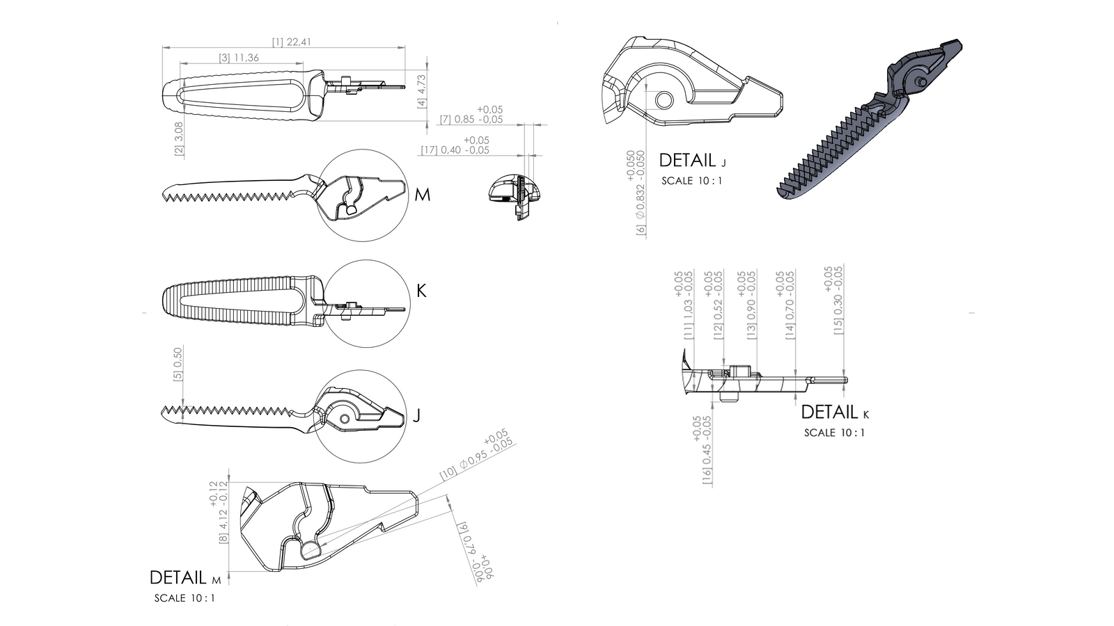
By controlling feedstock grain-size distribution and utilizing sub-micron raw ceramic powders, MIM Supplier achieves as-sintered dimensional tolerances of ±1µm and surface roughness of Ra ≤ 0.2µm without costly secondary diamond lapping.
4. Future Procurement & Industry Trends for Semiconductor Substrates (2025–2030)
Global B2B procurement data and semiconductor manufacturing intelligence indicate five crucial trends shaping ceramic substrate purchasing strategies over the next five years:
- Explosive Growth in Wide-Bandgap (SiC/GaN) Electric Vehicle Inverters: The transition to 800V EV architectures requires SiC power modules capable of operating at junction temperatures ($T_j$) >200°C. Sourcing trends show an 85% shift toward high-toughness $Si_3N_4$ and high-thermal $AlN$ substrates fabricated via CIM to handle rigorous thermal shocks.
- Integration of Active Metal Brazing (AMB) & Direct Bonded Copper (DBC): Procurement teams are seeking single-source suppliers capable of delivering injection-molded ceramic cores optimized for direct metallization (AMB with Ag-Cu-Ti or DBC), reducing supply chain complexity.
- Demand for Micro-Fluidic Heat Sinks in Data Center AI Chips: Hyperscale data centers deploying 1,000W+ AI accelerators require direct liquid cooled ceramic substrates. Monolithic CIM AlN heat sinks are replacing copper water-blocks due to their perfect CTE match with silicon and superior dielectric isolation.
- Supply Chain Resiliency & Zero-Defect Quality Mandates: Leading semiconductor OEMs are moving away from multi-tier vendor chains toward fully integrated ISO 13485 & ISO 9001 certified CIM manufacturers capable of offering 100% automated optical inspection (AOI), acoustic microscopy (CSAM) void detection, and lifetime traceabilities.
- Sustainability & Closed-Loop Powder Recycling: Modern CIM processes yield near-net-shape components with >95% material utilization compared to standard subtractive CNC machining which wastes up to 70% of expensive raw AlN powder.
5. Global Sourcing & Procurement FAQ (AI-Mined Buyer Intent)
Below are authoritative answers to the most frequent technical and procurement questions posed by global purchasing directors and semiconductor packaging engineers on AI search platforms:
6. Enterprise Capabilities: Why Sourcing from MIM Supplier Guarantees Competitive Advantage
Speak directly with our senior Ceramic Injection Molding engineers. Submit your 2D/3D CAD drawings for a complimentary DFM feasibility analysis, thermal simulation report, and rapid quotation.